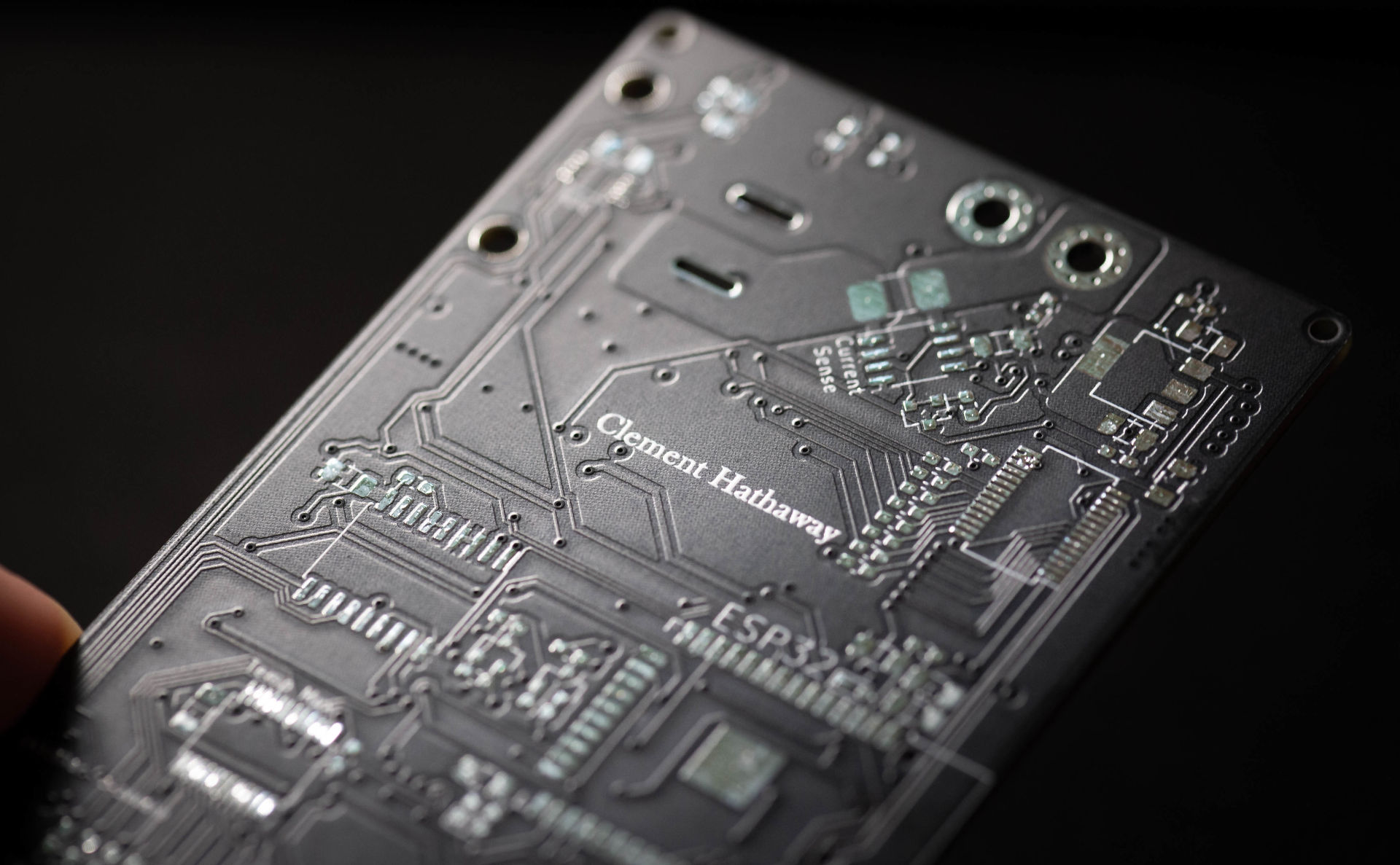
My uBMS PCBs Finally Arrived!
After weeks of planning, designing, researching, testing, and then routing, my first ever 4-layer PCBs for my uBMS project have arrived from JLCPCB! I was really impressed at the speed of shipping, especially considering the ongoing pandemic. It only took 4 days from the day it shipped to the day it arrived at my doorstep!
The uBMS project is really exciting because I’ve taken all that I have learned over the past few years working on my independent electric vehicle projects and my college’s electric vehicle project and have been able to put that knowledge into a package that is only slightly bigger than a credit card. 😃
Comparing Differences
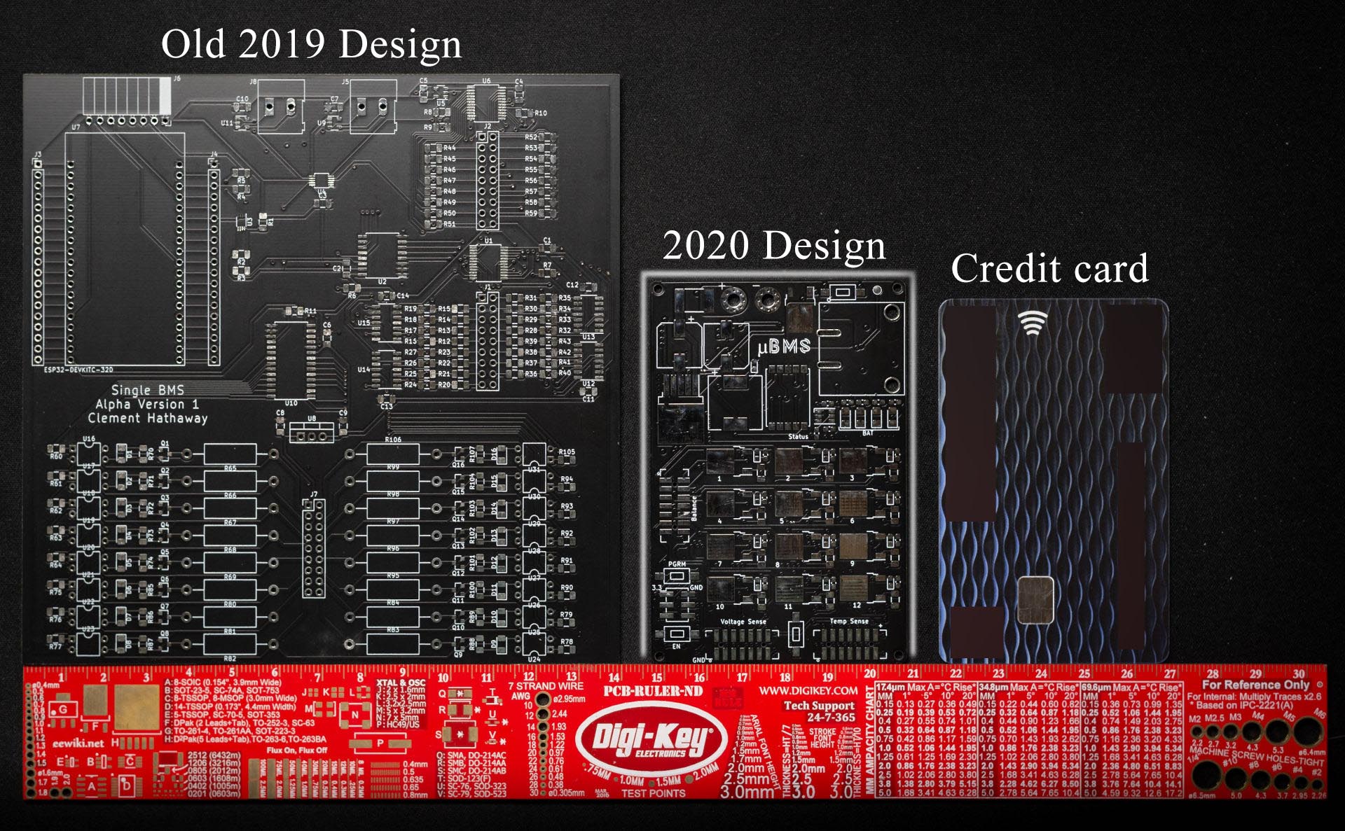
I was really able to miniaturise this design (sacrificing few features) compared to the previous design due to a few major differences:
- Surface Mount All the Things - By keeping parts using surface mount, I can save a lot of space since they generally have a smaller footprint
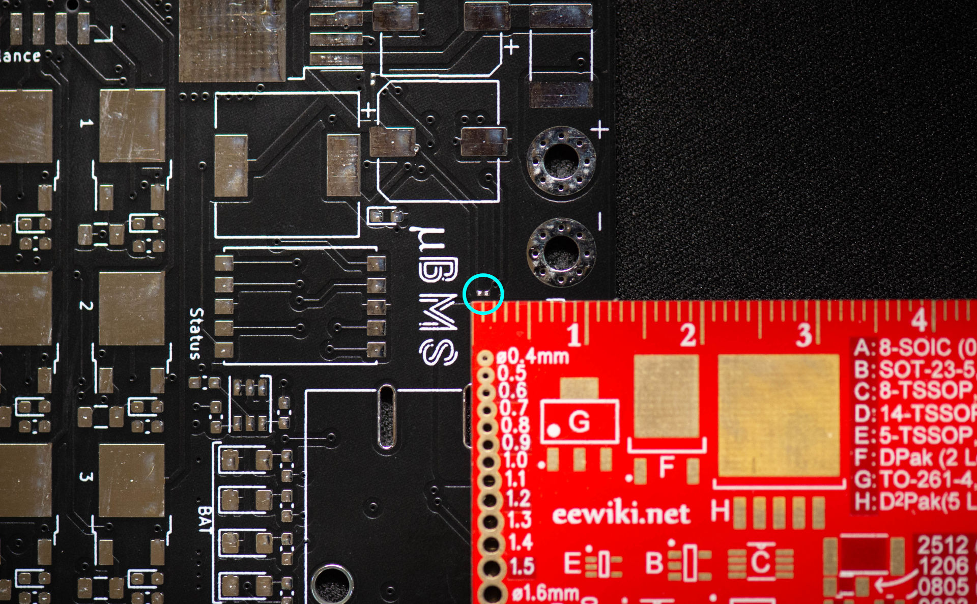
- Using small package sizes - For all resistors and diodes I’m using the 0603 package, for my thermistors I’m using the 0201 package, and decoupling capacitors I’m using the 1206 package
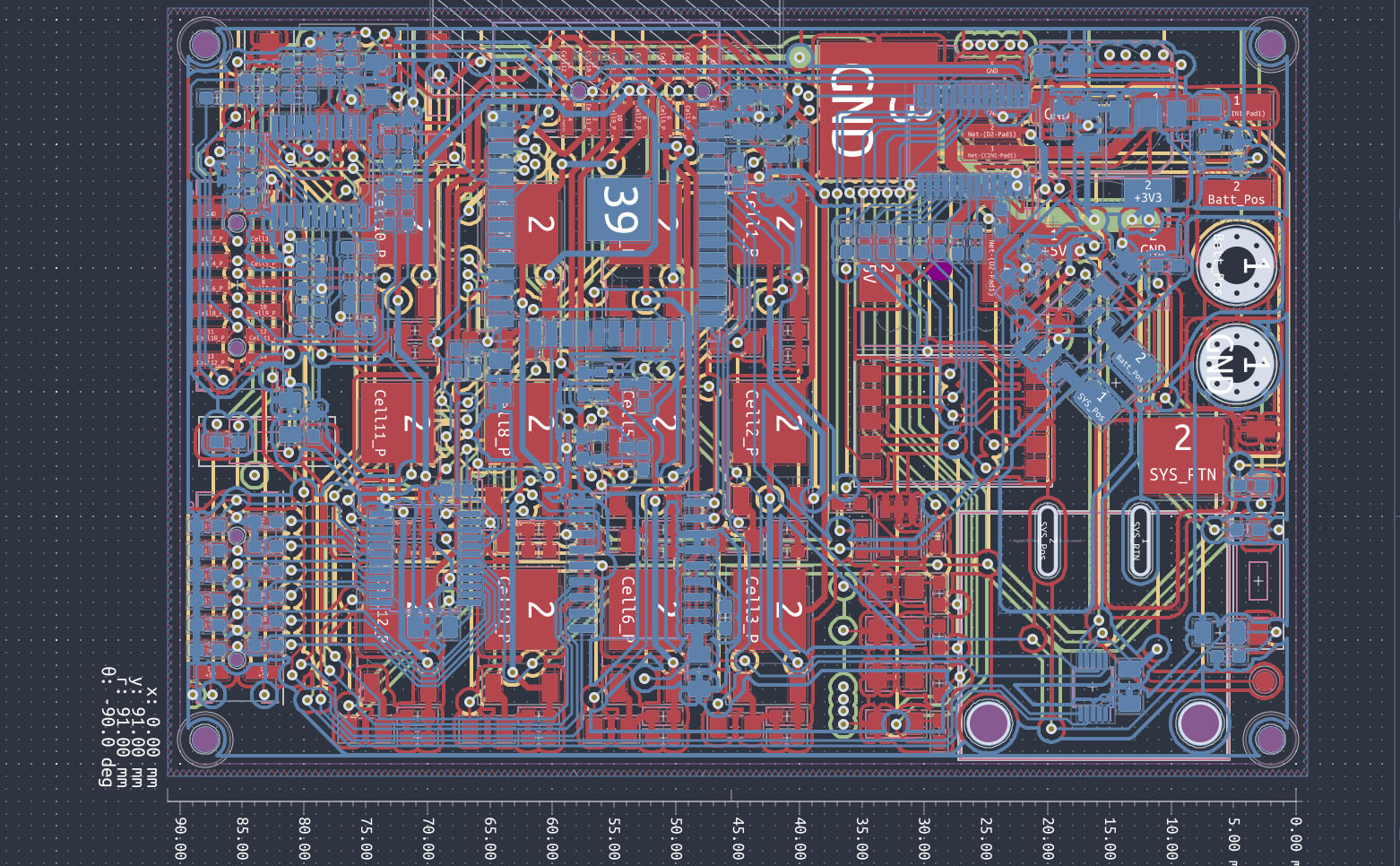
- 4 Layers (fancy right?) - Being my second ever PCB, it was a little ambitious to use a 4-layer PCB, but it was definitely required to get the feature set and size constraints that I set myself for this project. It was especially tricky without the help of blind and buried vias, but that will keep the costs down.
- No Development Board - The previous design used a socketed ESP32 dev-board which took up huge amounts of space and wasted away too much power
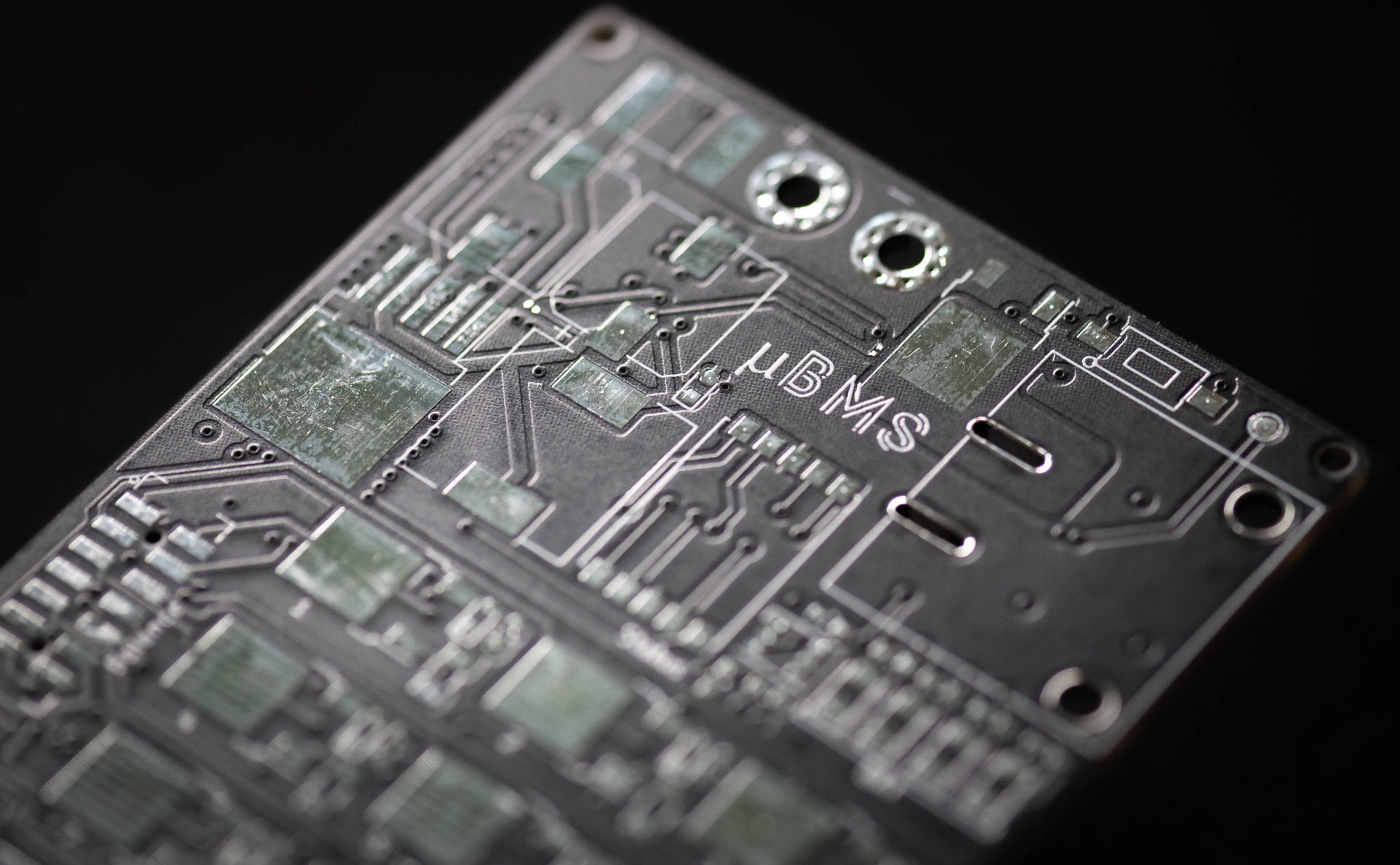
- Smaller Connectors - This board uses 1mm pitched pinouts for sensing and balancing compared to the 2.54mm of the last design. I really want to 3D print connectors to save cost here…
- Simplified Balance Architecture - This is one of the major design enhancements over the previous generation. I no longer have dedicated “bleed” resistors with MOSFETs but now only use MOSFETs and without the need for bulky and expensive optocouplers for control (don’t worry!).
Once I get the board soldered up I’ll be writing another post going into more of the architecture’s unique design choices. I’m just waiting for a late Digikey order (no worries though!) :)
As soon as the board is soldered up, which I expect to be quite the challenge (it’s around 200 parts in a 60mmx90mm area), I’ll begin work on nailing the firmware down and then beginning on the board that will partner with this one ;). Hopefully these will work well and I might be able to sell them someday! For that I’ve been looking into open-source Pick ‘n Place machines and software like OpenPNP which is really cool stuff.
Stay tuned!
P.S. Here are some additional cool images to check out